Program
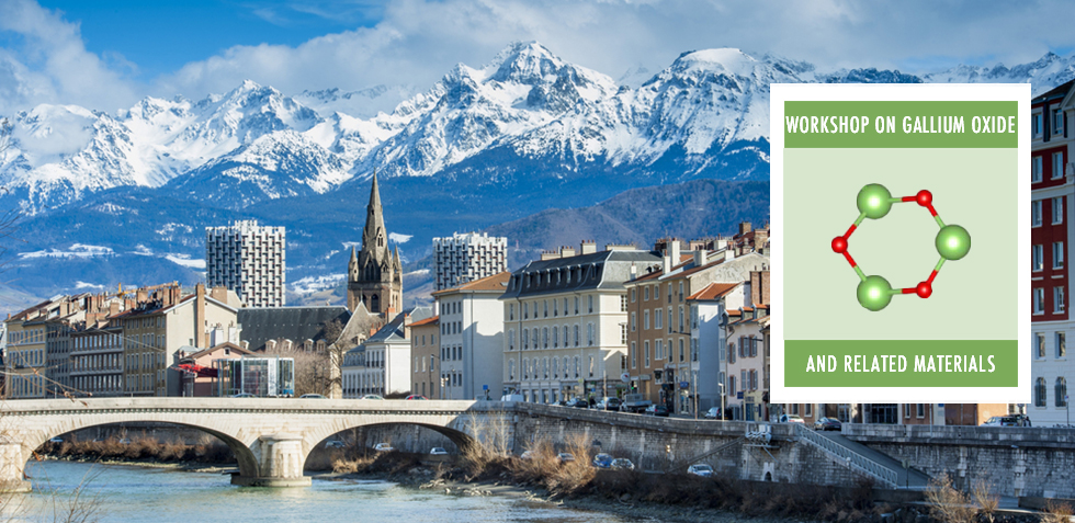
Workshop on Gallium Oxide and Related Materials
September 29-30, 2025
Salle des séminaires
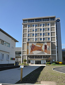
CNRS, Building A, 25 avenue des Martyrs, 38042 Grenoble
Program
Time
|
September 29, 2025
|
13:30 – 13:50
|
Workshop introduction
|
|
Growth and structural characterization 1
Chairman : Vincent Consonni (LMGP)
|
13:50 – 14:15
|
Andy Séguret
CEA-IRIG-PHELIQS & LMGP
|
ALD of epitaxial (002) κ-Ga2O3 thin films on c-plane sapphire
|
14:15 – 14:40
|
Ilyass Jellal
LMGP
|
κ- and β-phases of Ga2O3 thin films grown by atomic layer deposition: a study of their phase transition using thermal annealing
|
14:40 – 15:05
|
Alexandre Jaud
LMI
|
Ga₂O₃ thin films on c-plane Sapphire by Low-Pressure MOCVD. From Epitaxial Growth to Devices
|
15:05 – 15:30
|
Marielena Velasco-Enriquez
LMGP & Institut NEEL
|
Pulsed-Liquid Injection MOCVD of epitaxial Ga2O3 thin films
|
15:30 – 15:55
|
Julien Bosch
CEA-IRIG-PHELIQS
|
Plasma-Assisted Molecular Beam Epitaxy of β-Ga2O3/NiO Heterojunctions
|
15:55 – 16:25
|
Coffee break
|
|
Growth and structural characterization 2
Chairwoman : Ekaterine Chikoidze (GEMaC)
|
16:25 – 16:50
|
Vincent Consonni
LMGP
|
Ga2O3 Nanomaterials & Thin Films by Chemical Bath Deposition
|
16:50 – 17:15
|
Eva Monroy
CEA-IRIG-PHELIQS
|
Molecular Beam Epitaxy of Al-Polar Wurtzite AlN(0001) on β-Ga2O3(-201)
|
17:15 – 17:40
|
Enora Vuillemet
AMPERE
|
Raman and photoluminescence characterization of β-Ga2O3 for power electronic application
|
17:40 – 18:05
|
Marcin Konczykowski
LSI
|
Thermal Stability and Doping Effect of Electron Irradiation Induced Defects in β-Ga2O3 and GaN Crystals
|
|
Heterostructures
Chairwoman : Eirini Sarigiannidou (LMGP)
|
18:05 – 18:30
|
Adrien Roth
CEA-LETI & Institut NEEL
|
Investigating the blistering mechanisms of β-Ga2O3 under light ion implantation
|
18:30 – 18:55
|
Emilien Lefebvre
LMGP & Institut NEEL
|
Core Shell ZnO-Ga2O3 Nanowire Heterostructures for Piezoelectric Devices
|
18:55 – 21:00
|
Diner
|
Time
|
September 30, 2025
|
|
Electrical characterization
Chairman : Philippe Ferrandis (Institut Néel)
|
08:30 – 08:55
|
Ekaterina Chikoidze
GEMaC
|
The Beauty of Ga₂O₃ and ZnGa₂O₄ Electronic Properties
|
08:55 – 09:20
|
Akash Patnaik
GEMaC
|
Thin Film Deposition and Simulation of β-Ga2O3 Power Devices for High Voltage Applications
|
9:20 – 09:45
|
Ouissal Heribi
INL
|
A New Route to Efficient β-Ga₂O₃ p–n Junctions: Electrical and Defect Characterization of Phosphorus Ion Implantation
|
09:45 – 10:15
|
Coffee break
|
|
Technological steps and devices
Chairman : Jean-François Michaud (GREMAN)
|
10:15 – 10:40
|
Changzi Lu
AMPERE
|
Technology Optimization for a Ga2O3 power Schottky diode fabrication
|
10:40 – 11:05
|
Juan-Carlos Trujillo-Yague
Institut NEEL & LMGP
|
Optimization of Ti/Au Ohmic Contacts on β-Ga₂O₃
|
11:05 – 11:30
|
Philippe Ferrandis
Institut NEEL
|
Study of the Schottky barrier height distribution in β-Ga2O3 diodes
|
11:30 – 11:55
|
Tom Micottis
IEMN
|
Emerging Vertical Ga2O3 PiN Diodes for High-Power Conversion and Protection
|
11:55 – 12:20
|
Patrick PITTET
INL
|
New perspectives for the development of Ga₂O₃-based detectors for dosimetry in FLASH radiotherapy
|
12:20 – 13:50
|
Lunch
|
|
Short presentations
Chairman : Taoufik Slimani Tlemcani (GREMAN)
|
13:50 – 13:55
|
David Muñoz-Rojas
LMGP
|
New processes for the Spatial Atomic Layer Deposition (SALD) of functional materials: Ga2O3 from DMP-based non-pyrophoric precursors
|
13:55 – 14:00
|
Marty Volant
LMGP & CEA-IRIG-MEM
|
Advanced Transmission Electron Microscopy for optimization of gallium oxide thin films
|
14:00 – 14:05
|
Catarina Matos
LMGP & NOVA Lisboa
|
Heterostructures Made of Ga2O3 for self-powered UV photodetection and power electronics
|
14:05 – 14:10
|
Thomas Ribault
GEMaC/INSP
|
Ni₁₋ₓO/Ga₂O₃ Heterostructures for Next-Generation Power Electronics
|
14:10 – 14:15
|
Dimitri Bebien
GREMAN
|
Conception, realization and comparison of gallium nitride and gallium oxide based vertical power diodes
|
14:15 – 14:20
|
Vijay Thakur
LGP
|
Optimized Packaging of 10 kV Ga2O3 Power Module
|
14:20 – 15:00
|
Workshop conclusion
|
|